![]()
CBSE Guess > Papers > Important Questions > Class XII > 2011 > Physics > Physics By Mr. Ajay Sharma
CBSE CLASS XII
![]()
![]()
![]()
Semiconductor Physics
(Q.1) Define forbidden gap. ( 1 mark )
(Q.2) How does the energy gap in an intrinsic semiconductor change, when doped with a trivalent impurity? ( 1 mark ) (Q.3) Out of electrons and holes, which has higher mobility? ( 1 mark ) (Q.4) What is depletion region in a p-n junction? ( 1 mark ) (Q.5) Which special type of diode can act as a voltage regulator? Give the symbol of this diode and draw the general shape of its V-I characteristics. (H) ( 1 mark ) (Q.6) Draw the logic symbol of two input NOR gate. Write down its truth table. ( 1 mark ) (Q.7) What do you mean by rectification? ( 1 mark ) (Q.8) What is LED? ( 1 mark ) (Q.9) What is meant by the term doping? ( 1 mark ) (Q.10) What is an amplifier? ( 1 mark ) (Q.11) If a semiconductor has an intrinsic carrier concentration of 1.04 X 10¹⁴ /m3 when doped with 1028 /m3 phosphorous atoms, then the concentration of at room temperature will be (H) ( 1 mark )(a) 2 X 1028
(b) 1.04 X 10¹⁶ /m3
(c) 1.04 X 10¹⁴ /m3
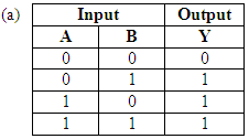
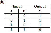
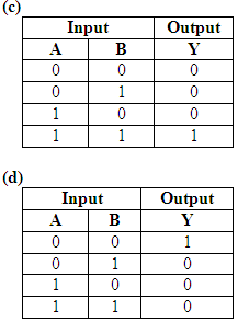
(d) 1.02 X 10¹⁴ /m3(Q.12) Which of the following truth table represents an AND gate? ( 1 mark )
(Q.13) In a half wave rectifier, the r.m.s value of the a.c component of the wave is ( 1 mark)
(a) equal to d.c value
(b) more than d.c value
(c) less than d.c value
(d) zero(Q.14) In a common base transistor circuit the current gain is 0.92 on changing emitter current by8.00 mA, the change in collector current is (H) ( 1 mark )
(a) 2.415 mA
(b) 7.36 mA
(c) 8.00 mA
(d) 0.92 mA(Q.15) Which of the following gate is considered as a universal gate? ( 1 mark )
(a) NOR gate
(b) AND gate
(c) NOT gate
(d) OR gate(Q.16) The output of a gate is '1' only when both inputs are '0'. The gate must be a ( 1 mark )
(Q.17) If a zener diode (Vz = 10V, Iz = 10 mA) is connected in series with a resistance and 20 V is applied across the combination, then the maximum resistance one can use without spoiling zener action is(H) ( 1 mark )
(Q.18) The current gain of a transistor is 100. If the base current changes by 200 mA. What will be the change in collector current? ( 1 mark )
(Q.19) The majority charge carriers in a p-type semiconductor are ( 1 mark )
(Q.20) A semiconductor is doped with a donor impurity ( 1 mark )
(a) the hole concentration decreases
(b) the hole concentration increases
(c) the electron concentration decreases
(d) the electron concentration remains unaffected(Q.21) If nh and ne are hole and electron concentrations then for an n-type semiconductor (H) ( 1 mark )
s
(Q.22) Zener diode is used for ( 1 mark )
(a) Rectification
(b) Stablization
(c) Amplification
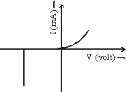
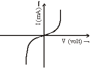
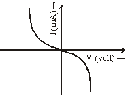
(d) Producing oscillations in an oscillator(Q.23) Which of the following graph represents the I-V characteristics of a zener diode? (H) ( 1 mark )
(a)
(b)
(c)
(d)
(Q.24) Which of the following is wrong for a transistor? (H) ( 1 mark )
(a) The ratio of change in collector-emitter voltage (DVCE) to the change in collector current (DIC) at a constant base current IB is called output resistance (r0).
(b) The ratio of change in base-emitter voltage (DVBE) to the resulting change in base current (DIB) at constant collector-emitter voltage (VCE) is known as input resistance (ri).
(c) The ratio of change in base current to the change in collector current is defined as the current amplification factor (b).
(d) A transistor acts as an amplifier when operated in the active region(Q.26) When the reverse potentials in the semiconductor diode are 10 V and 50 V, the corresponding reverse currents are 100 mA to 300 mA respectively. The reverse resistance of junction diode will be( 1 mark )
(Q.27) If the forward bias on p-n junction is increased from zero to 0.095 V, then no currunt flows in the circuit. The contact potential of junction plane is ( 1 mark )
(a) Zero
(b) 0.095 V
(c) More than 0.095 V
(d) Less than 0.95 V(Q.28) In case of p-n-junction diode, at zener voltage the current rises sharply. It happens because of ( 1 mark )
(a) High value of reverse bias
(b) Very low value of reverse bias
(c) Very high value of forward bias
(d) No reverse bias at all(Q.29) If A = 1 and B = 0, then in terms of Boolean algebra what is the value of A.A + B? ( 1 mark )
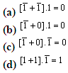
(Q.30) Which of the following is not true in Boolean algebra? (H) ( 1 mark )
(Q.31) A transistor has an α = 0.95 then b is equal to ( 1 mark )
(Q.32) An n-type and a p-type silicon can be obtained by doping pure silicon with ( 1 mark )
(a) sodium and magnesium
(b) phosphorus and boron
(c) boron and phosphorus
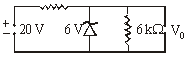
(d) indium and phosphorus(Q.33) What is the value of output voltage in the circuit below (H)
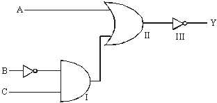
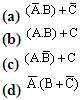
(Q.34) The output of the logic circuit shown in the figure below is best represented by which of the following options
(Q.35) What are the minority carries in a p-type semiconductor? ( 1 mark )
(Q.36) Resistivity of semiconductor depends on ( 1 mark )
(a) Shape of semiconductor
(b) Length of semiconductor
(c) Atomic nature of semiconductor
(d) Shape and nature of semiconductor(Q.37) In a common emitter circuit, if VCE is changed by 0.5 V, collector current Changes by 0.002 mA. What is the output resistance? ( 1 mark )
(Q.38) A common emitter circuit has an input resistance of 1.3 kilo-ohm and output resistance of 50 kilo-ohm. If the current gain is 65, what is the voltage gain? (H) ( 1 mark )
(Q.39) The electrical circuits used to get smooth D.C. output from a rectified circuit is called- ( 1 mark )
(a) Oscillator
(b) Full wave rectifier
(c) Amplifier
(d) Filter(Q.40) The potential difference across the collector of a transistor, used in common emitter mode is 1.5V, with the collector resistance of 3K Ω . Find
(i) the emitter, and
(ii) the base current, if the d.c. gain of the transistor is 50. (H) ( 2 Marks )(Q.41) Give any two differences between a half-wave rectifier and a full-wave rectifier. ( 2 Marks )
(Q.42) Transistor is a temperature-sensitive device. Explain. ( 2 Marks )(Q.44) Discuss how the OR gate is realized from the NOR gate. ( 3 Marks )
(Q.45) Why is the base region of a transistor usually made thin?In a common emitter mode of transisitor,d.c. current gain is 20, the emitter current is 7 mA. Calculate(i) base current, and
(Q.46) The input resistance of a silicon transistor is 665 Ω . Its base current is changed by 15 μ A, which results in change of collector current by 2mA. This transistor is used as a common emitter amplifier with a load resistance of 5 k Ω . Calculate
(ii) collector current. (H) ( 3 Marks )(i) current gain β0,
(Q.47) Draw the energy band diagram of a p-type semiconductor. Distinguish between p-type and n-type semiconductor.(3Marks ) (Q.48) Write the logic symbol and truth table of an AND gate. ( 5 Marks ) (Q.49) Draw a circuit diagram to obtain the characteristics of a n-p-n transistor in common emitter configuration. Describe how you will obtain input and output characteristics. Give shape of the curves.
(ii) transconductance gm, and
(iii) voltage gain Av of the amplifier. (H) ( 3 Marks )
![]()
![]()
![]()
Submitted By Mr. Ajay Sharma
Email Id : [email protected]